Research
AI and MBE Automation
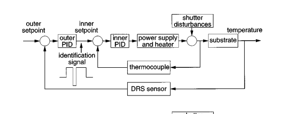
We demonstrated a closed-loop real-time-control of MBE growth using feed-back from an in-situ spectroscopic ellipsometer (SE) and a large material data base, which enabled precise control of layer thickness and alloy composition within one run without the need of ex situ characterization. The dynamic optical constant (OC) database developed for composition control of InGaAs and…

II-VI Semiconductor Solar Cells
J.-J. Li, L. et al., Applied Physics Letters 101, 061915-061915. (2012) CdSe/CdTe type-II superlattices grown on GaSb substrates by molecular beam epitaxy are studied using time-resolved and steady-state photoluminescence (PL) spectroscopy at 10 K. A carrier lifetime of 188 ns is observed in time-resolved PL measurements. The steady-state PL peak position exhibits a blue shift…

Multijunction solar cell testing
S. H. Lim, et al., Progress in Photovoltaics: Research and Applications, (2011). The effects of luminescence coupling on the external quantum efficiency (EQE) measurement of an InGaP/InGaAs/Ge triple junction solar cell were investigated. A small signal model was used to study the interaction of the subcells during EQE measurement. It was found that an optical–electrical…
GaAs high efficiency ultrathin film solar cells
W. Yang, et al., J. Appl. Phys. 115, 203105 (2014). This paper reports the proposal, design, and demonstration of ultra-thin GaAs single-junction solar cells integrated with a reflective back scattering layer to optimize light management and minimize non-radiative recombination. The structure of the demonstrated solar cells consists of an In0.49Ga0.51P/GaAs/In0.49Ga0.51P double-heterostructure PN junction with an…
Theory
D. Ding, et al., J. Appl. Phys. 110, 123104 (2011). A semi-analytical model is constructed for single- and multi-junction solar cells. Four typical planar structures with the combinations of a smooth/textured top surface and an absorbing/reflecting substrate (or backside surface) are investigated. The below-bandgap tail absorption increases the short-circuit current but decreases the output and…

Type-II Superlattice Semiconductors for Infrared Photodetectors
Type-II Superlattice Semiconductors for Infrared Photodetectors E. H. Steenbergen, et al., Appl. Phys. Lett. 99, 251110 (2011). Time-resolved photoluminescence measurements reveal a minority carrier lifetime of >412 ns at 77 K under low excitation for a long-wavelength infrared InAs/InAs0.72Sb0.28 type-II superlattice (T2SL). The considerably longer lifetime is attributed to a reduction of non-radiative recombination centers with the…
Heterovalent Semiconductor Structure: MBE growth and characterization
MBE growth of various kinds of III-V and II-VI compound semiconductors. A unique twin-chamber MBE system allows growth of any composition of III-V and II-VI alloys. Monolithic intergration material platform for various optoelectronic and electronic device applications. he II-VI chamber is capable of growing almost all possible combinations of materials including Zn, Se, Te, Mg,…
LEDs and Electroluminescence Refrigeration
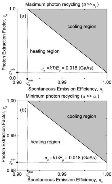
Photon extraction factor vs spontaneous emission efficiency for the maximum photon recycling case in a and for the minimum photon recycling case in b. The cooling efficiency is positive in the shaded area and zero along the solid line. The ideal cooling coefficient ic=kT/Eg used is for the GaAs band gap energy. 04 J.-B….
Two Color Detectors
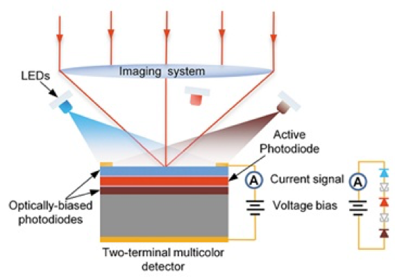
E. H. Steenbergen, et al. Appl. Phys. Lett. 97 161111-161114 (2010). A two-terminal multicolor photodetector that is most advantageous for greater than two bands is proposed. Individual color detection is realized with appropriate optical biasing. This concept is demonstrated experimentally using a three-color photodetector and biasing light emitting diodes. The measured linear dynamic range is…