Research

Low-Temperature Contact Formation for Photovoltaic Applications
Low resistance ohmic contacts are tremendously important for optoelectronic applications of all types. Formation of such contacts often requires high temperature (> 400°C) annealing to either form an alloy between the metal-semiconductor interface or to evaporate conductivity-limiting organics suspended in conductive pastes. Formation of low resistance ohmic contact readily at lower temperatures can broaden optoelectronic…
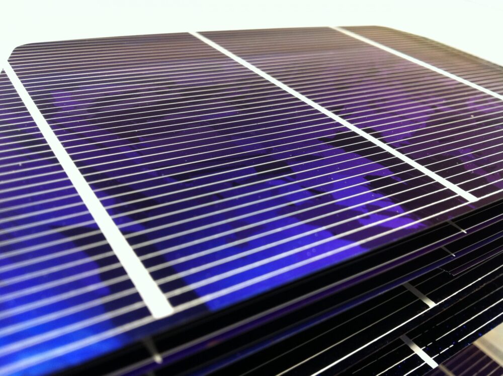
New carrier-selective contact materials for silicon solar cells
Current record crystalline silicon conversion efficiency of 25.6% is still about 3.5% away from its thermodynamic limit. Losses are principally attributed to parasitic optical absorption and carrier recombination, both related to the properties of the contact materials interfacing directly crystalline silicon. Thus, one approach to lead silicon solar cells to an efficiency breakthrough tackles the…
Silicon Defect Assessment and Modeling in High Quality c-Si Material
In the last few years research on silicon photovoltaic has strongly shifted toward high-quality mono-crystalline silicon material driven by the need of improving the efficiency/costs ratio. An effective way to study the detrimental defects in silicon wafers is by means of Temperature- and Injection-Dependent Lifetime Spectroscopy (TIDLS) coupled with the Shockley–Read–Hall recombination model. Given its…
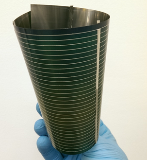
Cu(In,Ga)Se2 – Absorber layers
Chalcogenide-based solar cells are receiving attention because of their low manufacturing costs and demonstrated ~20% efficiency in laboratory-scale small-area devices. Theoretically, these devices should be capable of 30.5% efficiency, according to the Shockley–Queisser limit and, thus, surpass DOE’s SunShot goals for cost-competitive solar power. To date, however, CIGS modules have not surpassed 15 % efficiency, and incremental…

Transparent Conductors
Conductivity and transparency are two properties mutually exclusive in nature. Thus, transparent conductors are complex engineered systems that required fine levels of defect control and tuning. The basic requirements for TCOs have been covered by many authors but were originally presented by Hamberg and Granqvist: The first requirement is a host oxide with a band…
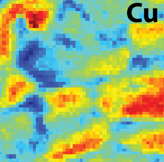
In-situ X-ray Microscopy
Our goal is to address the following industrially relevant effects : (1) Operando electromigration of species of species to grain boundaries, dislocations and interfaces (2) Metastable defects observed in CIGS after illumination and/or applied bias voltage (3) Nanoscale phase segregation as a function of growth conditions (4) Phase decomposition and interlayer diffusion as a function…

PVMirror Project
In the PVMirror project, we combine the technique of Photovoltaic and CSP(Concentrated Solar Power) together. Generally speaking, a band-pass mirror film is encapsulanted in front of solar cell inside a curved PV module so that PVMirror could have 20% Photovoltaic efficiency in day time and 6 hours of dispatch electricity at night. The mirror film…