Research
Example hero paragraph text.
Here is our vision
Here is our method
Our research goal is to understand and observe the fundamental processes that govern the operation of emerging devices, through nanoscale analytical imaging and correlative metrology. This generates fundamental understanding to engineer improved materials for nanoelectronics.
We leverage a multidisciplinary approach to develop custom-built instrumentation, and design experiments that generate fundamental understanding between nanoscale physical and chemical phenomena with relevant device and materials properties.
Areas of interest, and active projects.
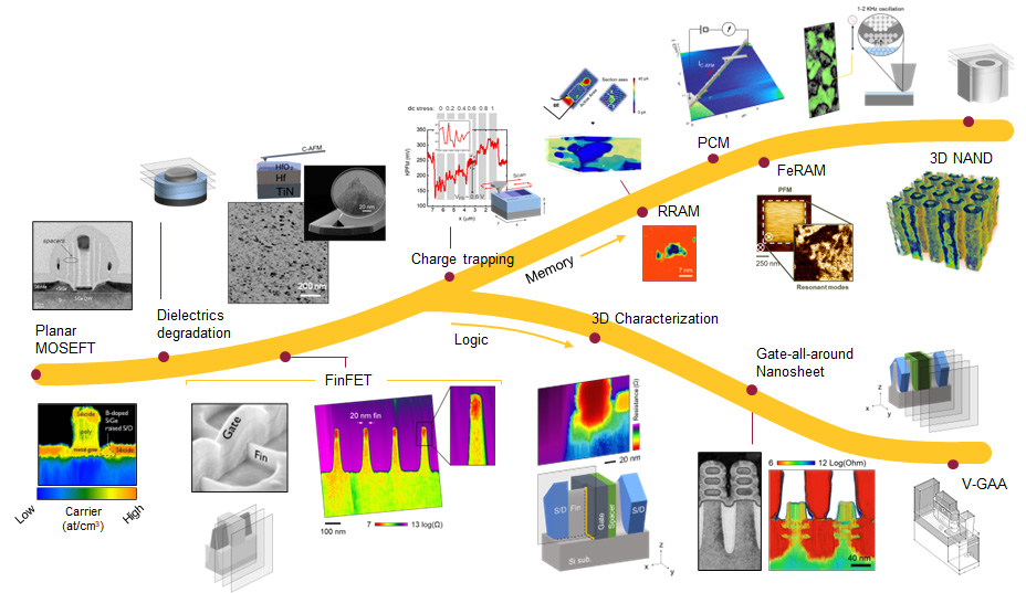
Reliability and Failure Analysis of Emerging Memory and Logic Devices
Materials analysis for emerging memory and logic devices.
At the intersection of condensed matter physics, semiconductor technology, and materials science, with a focus on nanoelectronics. We study fundamental processes that govern the operation of emerging devices, using nanoscale analytical instruments and correlative metrology to understand device physics, reliability, and failures.
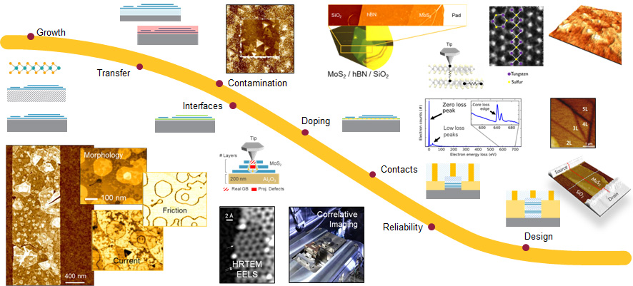
Metrology for 2D layered semiconductors
We strive to understands the interplay between electronic and structural properties in atomically-thin materials. We research for efficient screening methods in support of the process development of 2D semiconductors-based FETs.
This is pursued by a combination of microscopy and spectroscopy techniques, with emphasis on electrical scanning probe microscopies.
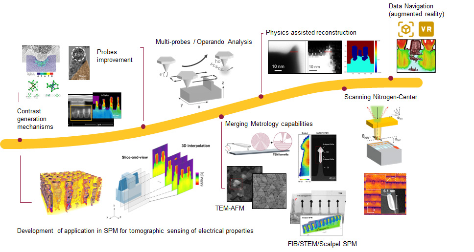
Instrumentation Development and Correlative Metrology
To understands the complex interplay between device physics and materials we often customize, or push, the limits of existing experimental methods. The co-localized analysis between device and materials is pursued via state-of-the-art instrumentation (in situ, operando) and by merging multiple analysis methods to gain access to multiple readouts in a correlative metrology analysis flow.